Loading...
Skip to content

Recent Works

    • About Taehwan
    • Publications
Two-dimensional chiral stacking orders in quasi-one-dimensional charge density waves

Two-dimensional chiral stacking orders in quasi-one-dimensional charge density waves

Posted on September 28, 2020December 8, 2020Publications

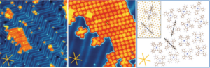
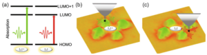
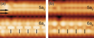
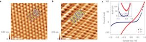
Chirality manifests in various forms in nature. However, there is no evidence of the chirality in one-dimensional charge density wave (CDW) systems. Here, we have explored the chirality among quasi-one-dimensional CDW ground states with the ...

Read more ⟶
Unusual Diffusion Behavior of Copper-Hexadecafluoro-Phthalocyanine Molecules on Au(111)

Unusual Diffusion Behavior of Copper-Hexadecafluoro-Phthalocyanine Molecules on Au(111)

Posted on August 11, 2020December 17, 2020Publications

The unusual bias-voltage dependence of copper-hexadecafluoro-phthalocyanine (F16CuPc) molecules on Au(111) was investigated by using scanning tunneling microscopy/spectroscopy (STM/STS) at low temperatures. Depending on the bias polarity, the molecules seem to cover the whole surface of ...

Read more ⟶
Tunable Plasmonic Quantum Light Source with Silver Nanoclusters on a Silver Surface

Tunable Plasmonic Quantum Light Source with Silver Nanoclusters on a Silver Surface

Posted on July 29, 2020December 17, 2020Publications

Scanning tunneling luminescence (STL) can be used to investigate the optical properties of nanostructures with high spatial resolution beyond the diffraction limit of light. To get appropriate STL spectra, one needs to modify the tip ...

Read more ⟶
Atomic structures of self-assembled epitaxially grown GdSi2 nanowires on Si(001) by STM

Atomic structures of self-assembled epitaxially grown GdSi2 nanowires on Si(001) by STM

Posted on February 4, 2019January 13, 2021Publications

Self-assembled rare-earth (RE) silicide nanowires (NWs) on semiconductor surfaces are considered as good candidates for creating and investigating one-dimensional electron systems because of their exceptionally anisotropic growth behavior and metallic property. While detailed atomic structures ...

Read more ⟶
Coplanar semiconductor–metal circuitry defined on few-layer MoTe2 via polymorphic heteroepitaxy

Coplanar semiconductor–metal circuitry defined on few-layer MoTe2 via polymorphic heteroepitaxy

Posted on September 18, 2017January 13, 2021Publications

Crystal polymorphism selectively stabilizes the electronic phase of atomically thin transition-metal dichalcogenides (TMDCs) as metallic or semiconducting, suggesting the potential to integrate these polymorphs as circuit components in two-dimensional electronic circuitry. Developing a selective and ...

Read more ⟶
Switching chiral solitons for algebraic operation of topological quaternary digits

Switching chiral solitons for algebraic operation of topological quaternary digits

Posted on February 6, 2017September 21, 2020Publications

Chiral objects can be found throughout nature1,2,3,4; in condensed matter chiral objects are often excited states protected by a system’s topology. The use of chiral topological excitations to carry information has been demonstrated, where the ...

Read more ⟶
Layer-Confined Excitonic Insulating Phase in Ultrathin Ta2NiSe5 Crystals

Layer-Confined Excitonic Insulating Phase in Ultrathin Ta2NiSe5 Crystals

Posted on August 15, 2016January 13, 2021Publications

Atomically thin nanosheets, as recently realized using van der Waals layered materials, offer a versatile platform for studying the stability and tunability of the correlated electron phases in the reduced dimension. Here, we investigate a ...

Read more ⟶
Chiral solitons in a coupled double Peierls chain

Chiral solitons in a coupled double Peierls chain

Posted on October 9, 2015September 21, 2020Publications

Chiral edge states are the hallmark of two- and three-dimensional topological materials, but their one-dimensional (1D) analog has not yet been found. We report that the 1D topological edge states, solitons, of the charge density ...

Read more ⟶
Visualization of the inverse layer-plus-island growth in Fe islands on W(110) substrate

Visualization of the inverse layer-plus-island growth in Fe islands on W(110) substrate

Posted on July 4, 2015September 21, 2020Publications

Many experiments have been conducted so far to control the growth mode in heterostructures, but success has only been restricted to strain-controlled growth systems. In this study, using the shadow mask deposition technique, we have ...

Read more ⟶
Charge-ordering cascade with spin–orbit Mott dimer states in metallic iridium ditelluride

Charge-ordering cascade with spin–orbit Mott dimer states in metallic iridium ditelluride

Posted on June 10, 2015September 21, 2020Publications

Spin–orbit coupling results in technologically-crucial phenomena underlying magnetic devices like magnetic memories and energy-efficient motors. In heavy element materials, the strength of spin–orbit coupling becomes large to affect the overall electronic nature and induces novel ...

Read more ⟶

Posts navigation

Older posts
Newer posts
Proudly powered by WordPress - Copyright © 2003-2025 | Theme: MiNNaK by Tamer Mancar