In-situ scanning tunneling microscopy observation of thickness-dependent air-sensitive layered materials and heterodevices
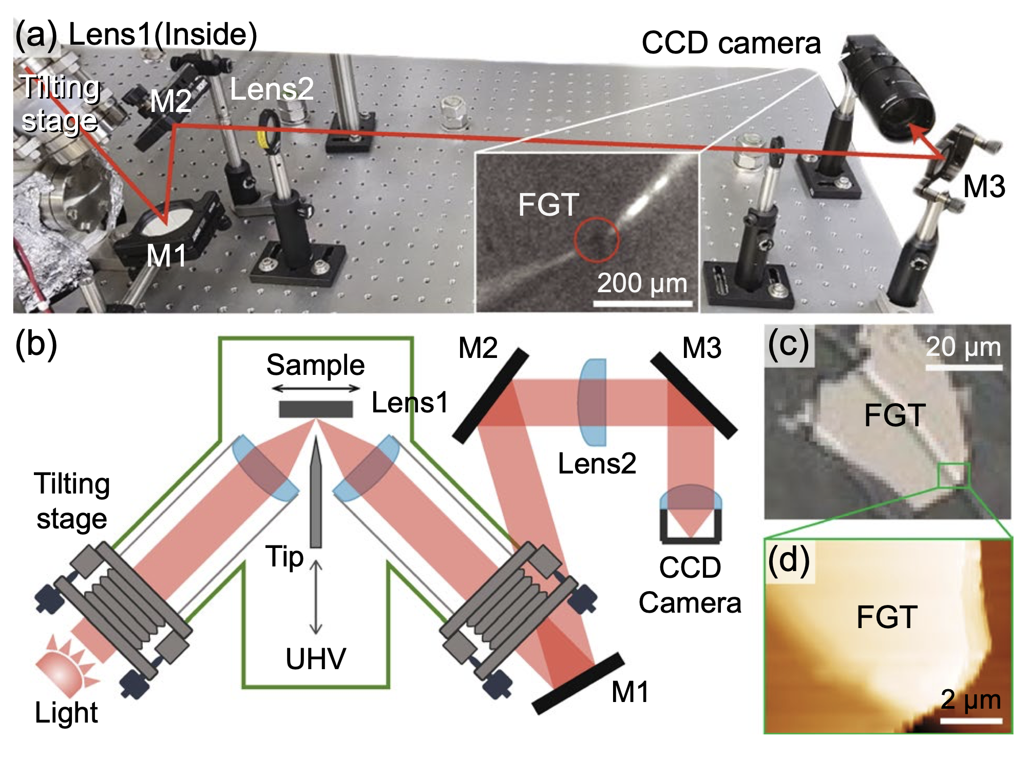
Quasi-two-dimensional (Quasi-2D) van der Waals (vdW) materials can be mechanically or chemically exfoliated down to monolayer because of their strong intralayer bonding and the weak interlayer vdW interaction. Thanks to this unique property, one can often find exotic thickness-dependent electronic properties from these quasi-2D vdW materials, which can lead to bandgap opening, emerging superconductivity, or enhanced charge density waves with decreasing thickness. Surface-sensitive scanning tunneling microscopy (STM) can provide direct observation of structural and electronic characteristics of such layered materials with atomic precision in real space. However, it is very challenging to preserve the intrinsic surfaces of air-sensitive quasi-2D materials between preparation and measurement. In addition, vdW 2D crystals after exfoliation are extremely hard to explore with a typical STM setup due to their small size (≤ 10 μm). Here, we present a straightforward method compatible with any STM setup having optical access: (1) exfoliating and/or stacking layered materials in a glove box, (2) transferring them to an ultra-high vacuum STM chamber using a suitcase without exposure to air, and (3) navigating surface to locate exfoliated vdW 2D flakes with different thicknesses. We successfully demonstrated that the clean surfaces of the air-sensitive Fe3GeTe2 can be effectively protected from unwanted oxidation during transfer. Furthermore, our method provides a simple but useful way to access a specific tiny stack of layered materials without any ex-situ fabrication processes for STM navigation. Our experimental improvement will open up a new way to investigate air-sensitive layered vdW materials with various thicknesses via surface-sensitive techniques including STM.
