Atomic structures of self-assembled epitaxially grown GdSi2 nanowires on Si(001) by STM
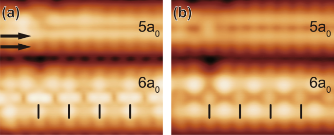
Self-assembled rare-earth (RE) silicide nanowires (NWs) on semiconductor surfaces are considered as good candidates for creating and investigating one-dimensional electron systems because of their exceptionally anisotropic growth behavior and metallic property. While detailed atomic structures are essential to understand electronic properties of these NWs, there have been only few successful observations of atomic structures with microscopy and reliable structure models are lacking. Here, we reinvestigate gadolinium silicide NWs with high resolution scanning tunneling microscopy (STM). We observe several different structures of Gd silicide NWs depending systematically on their widths, which consist of two distinct structural elements along the wires. The structure of a wide wire can be understood from that of a two dimensional silicide. Based on these STM observations, we propose new structure models of Gd silicide NWs.
