Polaronic Transport and Current Blockades in Epitaxial Silicide Nanowires and Nanowire Arrays
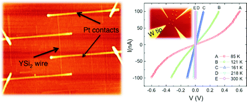
Crystalline micrometer-long YSi2 nanowires with cross sections as small as 1 × 0.5 nm2 can be grown on the Si(001) surface. Their extreme aspect ratios make electron conduction within these nanowires almost ideally one-dimensional, while their compatibility with the silicon platform suggests application as metallic interconnect in Si-based nanoelectronic devices. Here we combine bottom-up epitaxial wire synthesis in ultrahigh vacuum with top-down miniaturization of the electrical measurement probes to elucidate the electronic conduction mechanism of both individual wires and arrays of nanowires. Temperature-dependent transport through individual nanowires is indicative of thermally assisted tunneling of small polarons between atomic-scale defect centers. In-depth analysis of complex wire networks emphasize significant electronic crosstalk between the nanowires due to the long-range Coulomb fields associated with polaronic charge fluctuations. This work establishes a semiquantitative correlation between the density and distributions of atomic-scale defects and resulting current–voltage characteristics of nanoscale network devices.
